Bulky wearables frustrate users involved in sports or daily tasks. You want sleek devices, but hardware limits you. Miniaturization of RFID chips offers the solution.
Miniaturization allows engineers to embed RFID capabilities1 into rings, glasses, and fabrics without compromising comfort. However, this creates significant challenges regarding antenna design2, signal range3, and interference management4 that product designers must overcome to ensure reliability.

During my early days as a production line operator at Fongwah, I saw how difficult it was to fit standard components into small housings. We often had to reject designs because the casing was too tight for the chip. Now, as a Marketing Manager, I see the industry moving toward invisible technology. This shift is exciting, but it brings new headaches for engineers like you. Let's look at what this evolution really means for your next project.
What design freedoms do smaller RFID chips unlock?
Clunky designs scare away fashion-conscious consumers. Your product looks like a gadget, not an accessory. Tiny chips let you design true jewelry.
Smaller RFID footprints enable seamless integration into smart rings, eyewear, and medical patches. This allows for lighter, more discreet form factors that improve user comfort and aesthetic appeal while maintaining essential connectivity.

When we reduce the physical size of the RFID transponder, the constraints on the industrial design frame disappear. We can stop building the device around the chip and start fitting the chip into the vision.
Wearable Form Factors
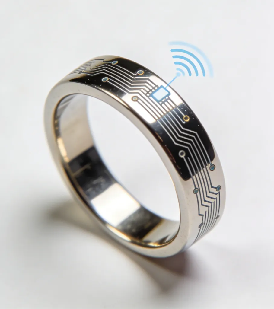
In the past, an RFID-enabled wristband had to be thick. Now, with miniaturized chips, we see "Smart Rings" and even "Smart Nails." I remember a client recently asking if we could put a tag inside a pair of sunglasses frames. Five years ago, I would have said no. Today, it is possible. This opens up high-value markets like luxury goods authentication and contactless payments in fashion items.
Advanced Textile Integration
Miniaturization allows for "E-textiles." Chips can be woven directly into fabric fibers. This is crucial for the healthcare sector. Patients can wear a shirt that tracks inventory or access control without a plastic hard tag. It feels like normal clothing.
| Application Area | Previous Constraint | New Opportunity |
|---|---|---|
| Smart Jewelry | Bulky bezels needed to hide chips. | Slim, elegant designs (Rings, Earrings). |
| Healthcare | Hard plastic wristbands caused irritation. | Soft, flexible smart patches on skin. |
| Sports Gear | Tags altered the aerodynamics of equipment. | Embedded chips with zero drag or weight. |
However, freedom comes with a price. As we shrink the package, we lose space for other components. This forces us to think critically about how we utilize every millimeter of the device.
How does size reduction affect antenna performance and signal integrity?
Tiny antennas often fail to catch enough energy. Your device looks great but reads poorly. You must innovate to save the signal.
Shrinking the device limits the physical space available for the antenna, which typically reduces the read range. Engineers must employ complex structural designs and high-permeability materials to compensate for the gain loss in these compact environments.
This is the area where my technical background usually clashes with pure designers. A designer wants the chip to be invisible, but as an engineer, I know that RF involves physics you cannot cheat.
The Resonance Problem
RFID relies on resonance. When you make an antenna smaller than its optimal wavelength, efficiency drops. For LF and HF systems, this is manageable but difficult. for UHF, it is a nightmare. I recall testing a prototype smart button where the read range dropped from 2 meters to 2 centimeters just because we shrank the housing by 10%.
Body Detuning Effects
The human body is mostly water. Water absorbs RF energy. When a miniaturized wearable sits directly on the wrist or finger, the "body effect" detunes the antenna. The resonant frequency shifts. To fix this, we need isolation layers or specialized ferrite sheets to direct the magnetic flux away from the skin.
Critical Engineering Solutions
We cannot just shrink the antenna design2. We have to change the geometry.
- 3D Antennas5: Using the z-axis (height) of the PCB to create a loop.
- Booster Antennas: Using the metal casing of the wearable itself as a signal booster.
- Ferrite Materials: Using high magnetic permeability sheets to concentrate the field.
| Technical Challenge | Cause | Potential Solution |
|---|---|---|
| Frequency Shift | Proximity to human skin/tissue. | Automated impedance tuning circuits. |
| Reduced Gain | Smaller physical aperture of the antenna. | Using active signaling (Battery Assisted). |
| Interference | Tight packing with batteries/screens. | Strategic component placement and shielding. |
What are the assembly challenges for miniaturized RFID wearables?
Handling microscopic parts leads to high defect rates. Your production costs skyrocket due to waste. Precision manufacturing is the only path forward.
Integrating tiny chips into flexible or curved wearable surfaces requires advanced bonding techniques like flip-chip or wire bonding. Manufacturers must also ensure the assembly can withstand mechanical stress6, moisture, and heat without damaging the delicate connections.

From my time managing a team, I know that the smaller the part, the harder it is to handle. Miniaturization7 changes the entire assembly line process. You cannot use standard pick-and-place machines for everything anymore.
Thermal Management and Bonding
Small chips have small pads. Standard soldering often creates bridges (short circuits). We see a shift toward Anisotropic Conductive Film8 (ACF) bonding or Ultrasonic bonding. These methods are precise but sensitive to heat. If the bonding temperature is too high, you damage the substrate. If it is too low, the connection fails after a week of use.
Mechanical Durability
A smart watch is rigid. A smart shirt or a flexible wristband bends. Miniaturized chips are brittle silicon. When you embed a tiny chip into a flexible band, mechanical stress6 concentrates on the connection points.
- The Failure Point: The connection between the chip and the antenna usually breaks first.
- The Fix: We use underfill epoxies to glue the chip down firmly. This distributes the stress.
Waterproofing (Ingress Protection)
Wearables face sweat, rain, and swimming pools. Sealing a miniaturized device is hard. There is no room for rubber gaskets. We rely on potting compounds9 (glues) to seal the electronics. However, some potting materials change the dielectric constant near the antenna. This brings us back to the tuning problem. You fix the waterproofing10, but you break the radio frequency.
| Assembly Risk | Description | Mitigation Strategy |
|---|---|---|
| Cold Solder Joints11 | Poor connection due to small pad size. | X-Ray inspection during QA. |
| ESD Damage12 | Static electricity destroys tiny circuits. | Strict ionizer controls in assembly. |
| Encapsulation Shift | Potting material detuning the antenna. | Pre-accounting for glue dielectric in design. |
Conclusion
Miniaturization enables sleek wearables but requires solving complex antenna and assembly hurdles. At Fongwah, we provide the quality RFID components you need to master this balance.
---Learn about the transformative impact of RFID on wearables and their applications in various industries. ↩
Understand the complexities of designing antennas for small devices and how they affect performance. ↩
Discover the relationship between device size and signal range, crucial for effective RFID functionality. ↩
Find out how to mitigate interference issues in compact devices for better performance. ↩
Understand the design and functionality of 3D antennas in enhancing device performance. ↩
Understand the impact of mechanical stress on wearables and how to mitigate it. ↩
Explore how miniaturization enhances device design and functionality, making technology more user-friendly. ↩
Learn about this advanced bonding technique and its significance in miniaturized electronics. ↩
Understand how potting compounds are used for sealing and protecting electronic components. ↩
Discover effective waterproofing techniques to enhance the durability of wearables. ↩
Learn about the issues related to cold solder joints and how to prevent them in manufacturing. ↩
Explore strategies to protect sensitive electronics from electrostatic discharge during assembly. ↩